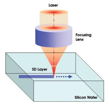
Dicing of silicon wafers may also be performed by a laser based technique the so called stealth dicing process.
Laser cutter for silicon wafer.
All that is required is a drawing to getting started.
However laser ablation has its own problems.
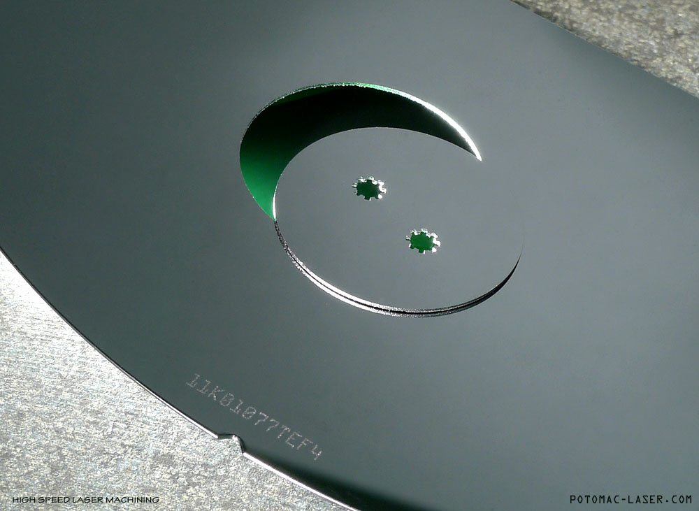
Demonstration of cutting features into 1 5 mm thick silicon wafers using a laser micromachining system equipped with a qcw laser.
The same system can be used to downsize larger silicon wafers for use in smaller format processing tools.
Sapphire silicon wafer cutter.
This is usually followed by a mechanical breaking procedure to produce silicon rectangular tiles for subsequent operations he mechanical break will follow allowing the scribing line offering the least path of resistance.
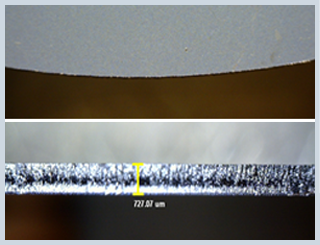
The figure shows 700 µm wafer downsizing top view and side view.
Due to the reflection it only made slight scratch and could not cut.
How is laser dicing silicon being processed.
Traditionally silicon wafers have been cut with diamond saws occasionally using a scribe and break process which have the limitation that they can only cut straight lines and suffer from edge chipping and frequency doubled vanadate lasers which are both slow and expensive to operate as is the microjet process.
Solutions are available for machining smaller diameter wafers from larger ones solar cell downsizing or silicon stencil cutting.
Cut features are round holes with no cracking or rough edges.
Laserod has a division that focuses on the building and integration of a full line of fiber laser micromachining equipment and a diode that can be used for laser dicing silicon wafer resistor trimming scribing substrates of silicon and alumina and cutting thin plastics and metals.
This lines introduces regions of weakness.
Scribing causes partial cut lines on the wafer.
Material thickness up to 1mm.
For silicon wafers less than 100 μm thick laser ablation offers an alternative to the blade technique which is too powerful for the delicate thin wafers.
Blackstar is a wafer dicing system utilizing fantom width laser dicing technology fwldt invented and patented by laser photonics and modified to accommodate the requirements of a silicon wafer singulation process without affecting the existent dicing method processes or procedures.
It works as a two stage process in which defect regions are firstly introduced into the wafer by scanning the beam along intended cutting lines and secondly an underlying carrier membrane is expanded to induce fracture.
We tried cutting a silicon wafer with fabool laser mini 1 6w and 3 5w model.